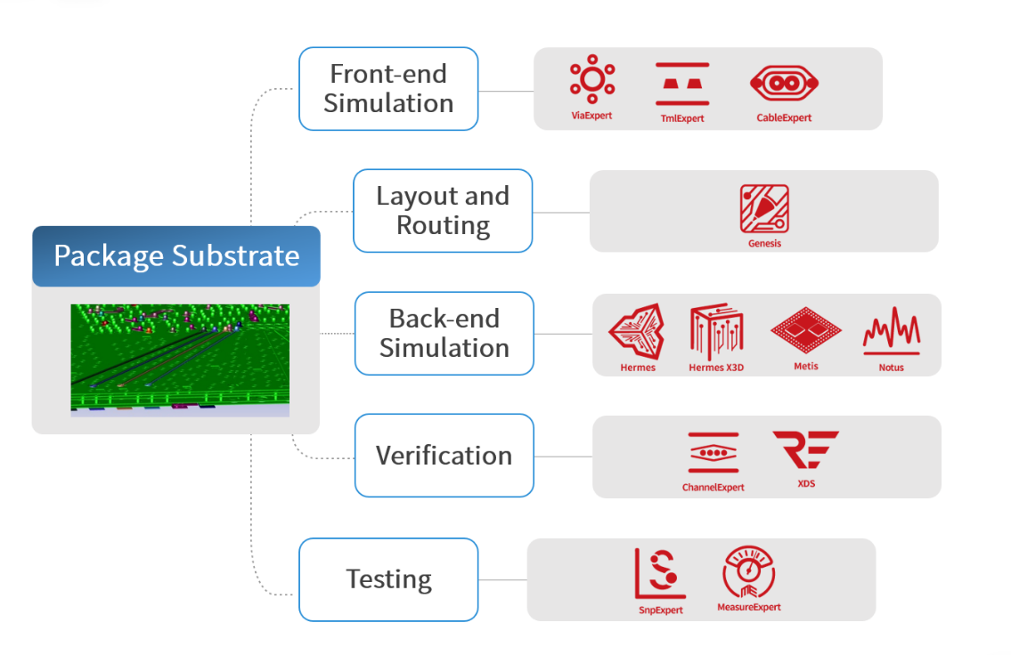
Package Substrate
Background

As a major packaging and PCB manufacturing country, domestic manufacturers bear 50% of the world's packaging and testing+ PCB scale. Many companies' design tools have their own rule frameworks and processes, to output data which meets IPC standards and industrial production process capabilities. With the increasing complexity and performance of electronic system design, coupled with the rapid development of integrated circuit process and packaging technology, driven by the system modular design concept and the open-source trend of software and hardware, the design and development cycle of board-level products in multiple fields is getting shorter, demand for the reuse of design rule constraints is increasing. Depending on product complexity, the design constraints that need to be followed in different fields are also different, which often requires numerous auxiliary tools customized for processes and businesses. In this series of processes, users mainly face the following major pain points:
1. For different products, it is difficult to balance the flexibility and comprehensiveness of design tool rules and over 200 check items. Design tools under the traditional CS architecture are usually large and complex, struggling to adapt complex and changing product forms, and keep pace with changes in manufacturing processes.
2. From design, simulation, DFX, and other single-domain, multi-platform collaboration leads to numerous design iterations and the turnaround time is at least two weeks; the user interface is complex, and the learning and transition costs are high. The interaction frequency is high for tools in a fully integrated environment that encompasses chip, package, and board level, making the processes difficult to merge.
3. Models and existing design data are scattered and difficult to maintain and reuse. Cross-platform design faces challenges in unifying data formats, synchronization, output, and conversion, along with the risks of non-standard data not being supported and loss of precision.
4. There's a lack of a customized development environment that supports mainstream general-purpose programming languages, making secondary development and customization challenging. The resources for vendor development support are limited, and needs are easily ignored.
Solution

Xpeedic‘s Genesis is a big data simulation-driven, software-defined schematic, PCB, and 2.5/3D packaging design platform with interactive semi-automatic routing capabilities. Genesis offers a comprehensive and complete solution. In terms of schematic diagrams, it supports the design of common single-unit and multi-unit schematic symbols, allows for rapid retrieval and reuse through a symbol library, and enables quick multi-pin editing through template import. It also supports layout and simulation of critical attribute settings. The tool allows for the creation of both simple and complex hierarchical circuit schematics, and supports convenient and quick modular definition as well as flexible settings for ports, power supply, voltage drop, noise, and other metrics. The integrated multi-functional netlist supports PCB synchronization, is compatible with multi-platform netlists, and efficiently integrates functions for paginated and modular automatic interactive layout and simulation requirements synchronization.

